Glass Wafer · TGV Substrates
Core Materials for Chip Packaging
From precision glass wafer processing to TGV substrates, SEMI-compliant and built for 5G/6G RF modules, AI packaging (CoWoS/HBM), and MEMS sensors — with one-stop optical coating included.
Three Size Options
SEMI Standard
Custom Sizes
Low-Loss Substrate
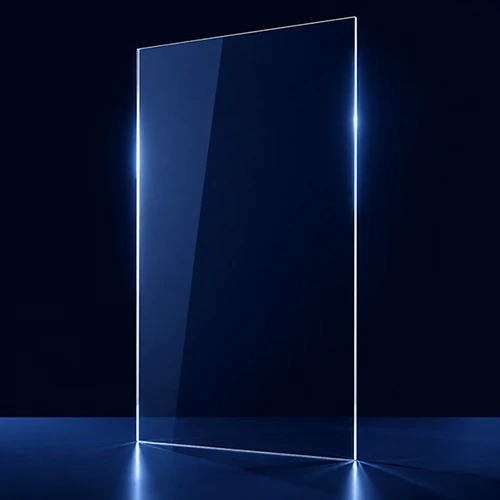
Glass Wafer · TGV Substrates
Core Materials for Chip Packaging
From precision glass wafer processing to TGV substrates, SEMI-compliant and built for 5G/6G RF modules, AI packaging (CoWoS/HBM), and MEMS sensors — with one-stop optical coating included.
Three Size Options
SEMI Standard
Custom Sizes
Low-Loss Substrate
TGV Glass Substrates
Next-Generation Packaging Interconnects
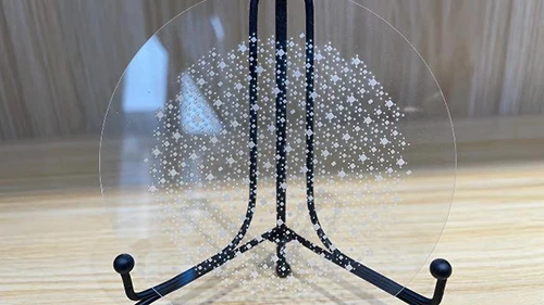
Through Glass Via (TGV) replaces traditional silicon substrates with low-loss glass, delivering superior electrical insulation, lower dielectric loss, and higher integration density. As demand surges for 5G mmWave, AI high-performance computing packaging, and MEMS sensors, TGV is becoming an essential material for advanced packaging.
- Via Diameter30 – 150 μm
- Via Pitch50 – 500 μm
- Substrate Thickness0.1 – 0.7 mm
- Dielectric Constant (1GHz)< 6
- Coefficient of Thermal Expansion (CTE)3 – 7 ppm/°C
- Key Applications5G/6G · AI Packaging · MEMS
TGV Glass Substrates
Next-Generation Packaging Interconnects
Through Glass Via (TGV) replaces traditional silicon substrates with low-loss glass, delivering superior electrical insulation, lower dielectric loss, and higher integration density. As demand surges for 5G mmWave, AI high-performance computing packaging, and MEMS sensors, TGV is becoming an essential material for advanced packaging.
- Via Diameter30 – 150 μm
- Via Pitch50 – 500 μm
- Substrate Thickness0.1 – 0.7 mm
- Dielectric Constant (1GHz)< 6
- Coefficient of Thermal Expansion (CTE)3 – 7 ppm/°C
- Key Applications5G/6G · AI Packaging · MEMS
Where It's Used
From advanced semiconductor packaging to precision optical instruments, supporting a wide range of high-tech manufacturing needs.

TGV substrates are used in 5G mmWave RF front-end modules (RFFE), CoWoS packaging for AI accelerators, and high-bandwidth memory (HBM), meeting the demands of high-density interconnects and low-loss transmission — a key material for AI computing infrastructure.

Precision glass wafers are widely used in MEMS pressure sensors, gyroscopes, camera lens optical components, medical diagnostic instruments, and aerospace sensing systems — maintaining high reliability even under extreme heat, pressure, and vibration.
Where It's Used
From advanced semiconductor packaging to precision optical instruments, supporting a wide range of high-tech manufacturing needs.
TGV substrates are used in 5G mmWave RF front-end modules (RFFE), CoWoS packaging for AI accelerators, and high-bandwidth memory (HBM), meeting the demands of high-density interconnects and low-loss transmission — a key material for AI computing infrastructure.
Precision glass wafers are widely used in MEMS pressure sensors, gyroscopes, camera lens optical components, medical diagnostic instruments, and aerospace sensing systems — maintaining high reliability even under extreme heat, pressure, and vibration.
Specialty Optical Glass Processing
Custom processing services for Carrier Glass, piezoelectric materials, Blue Glass, and a wide range of optical glass types.
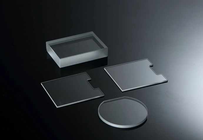
Supports ultra-thin wafers (≤150μm) during thinning, coating, and etching processes to prevent breakage — cleanable and reusable afterward to reduce production costs.
| Specifications | |
|---|---|
| Available Sizes | 6" / 8" / 12" |
| Material | Fused Silica / BF33 |
| Thickness | 500μm – 775μm |
| TTV | ≤1μm (premium) / ≤2μm |
| Surface | DSP double-side polished, Ra ≤0.5nm |
| Heat Resistance | Fused Silica >1000°C |
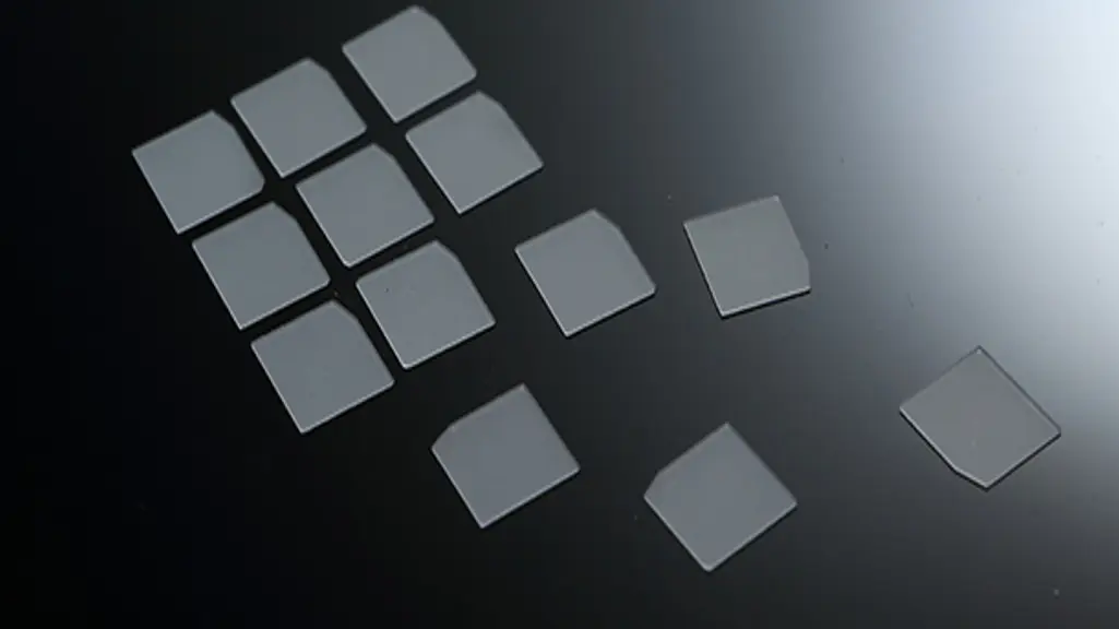
Made from synthetic quartz and available in plano, plano-convex, and bi-convex cut forms, suitable for high-reliability applications in aerospace, telecom base stations, and satellites.
| Specifications | |
|---|---|
| Material | Synthetic Quartz |
| Size | φ4.5–φ14mm / 1.8×3–30×30mm |
| Frequency | 5MHz (O3) – 120MHz (O5) |
| Cut Type | Plano / Plano-convex / Bi-convex / Doubly rotated cut |
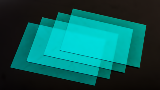
Blocks infrared light above 700nm to ensure accurate color reproduction on CMOS sensors, widely used in smartphone camera modules, automotive lenses, and security surveillance.
| Specifications | |
|---|---|
| Material | SCHOTT BG / CDGM QB / NEG |
| Size | 77×77mm (standard) |
| Thickness | 0.11 / 0.145 / 0.21 / 0.3mm |
| Cutoff Wavelength | >700nm IR blocking |
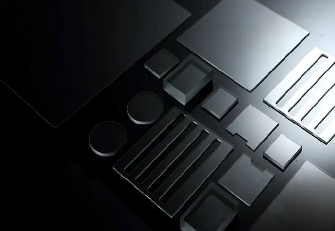
Precision cutting, grinding, and polishing services for optical glass from multiple leading brands, covering applications from camera lenses to medical instruments.
| Material | Application |
|---|---|
| SCHOTT B270 / D263T | High-transmission optics |
| JGS1 (Fused Silica) | UV optics |
| OHARA Series | Camera, medical |
| CORNING Eagle XG | TFT-LCD substrates |
Specialty Optical Glass Processing
Custom processing services for Carrier Glass, piezoelectric materials, Blue Glass, and a wide range of optical glass types.
Supports ultra-thin wafers (≤150μm) during thinning, coating, and etching processes to prevent breakage — cleanable and reusable afterward to reduce production costs.
| Specifications | |
|---|---|
| Available Sizes | 6" / 8" / 12" |
| Material | Fused Silica / BF33 |
| Thickness | 500μm – 775μm |
| TTV | ≤1μm (premium) / ≤2μm |
| Surface | DSP double-side polished, Ra ≤0.5nm |
| Heat Resistance | Fused Silica >1000°C |
Made from synthetic quartz and available in plano, plano-convex, and bi-convex cut forms, suitable for high-reliability applications in aerospace, telecom base stations, and satellites.
| Specifications | |
|---|---|
| Material | Synthetic Quartz |
| Size | φ4.5–φ14mm / 1.8×3–30×30mm |
| Frequency | 5MHz (O3) – 120MHz (O5) |
| Cut Type | Plano / Plano-convex / Bi-convex / Doubly rotated cut |
Blocks infrared light above 700nm to ensure accurate color reproduction on CMOS sensors, widely used in smartphone camera modules, automotive lenses, and security surveillance.
| Specifications | |
|---|---|
| Material | SCHOTT BG / CDGM QB / NEG |
| Size | 77×77mm (standard) |
| Thickness | 0.11 / 0.145 / 0.21 / 0.3mm |
| Cutoff Wavelength | >700nm IR blocking |
Precision cutting, grinding, and polishing services for optical glass from multiple leading brands, covering applications from camera lenses to medical instruments.
| Material | Application |
|---|---|
| SCHOTT B270 / D263T | High-transmission optics |
| JGS1 (Fused Silica) | UV optics |
| OHARA Series | Camera, medical |
| CORNING Eagle XG | TFT-LCD substrates |
Quality Inspection Equipment
Equipped with professional optical measurement instruments to ensure every glass substrate meets the strictest quality standards in the semiconductor and optics industries.
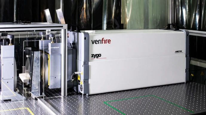
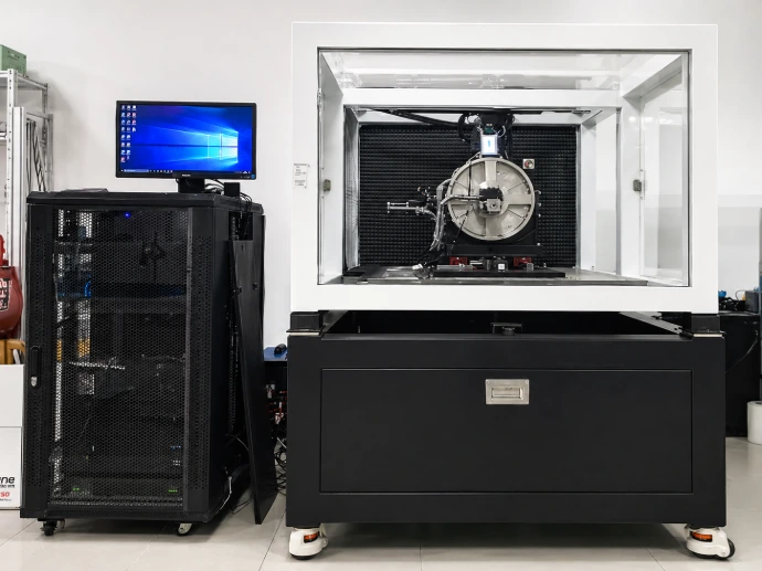
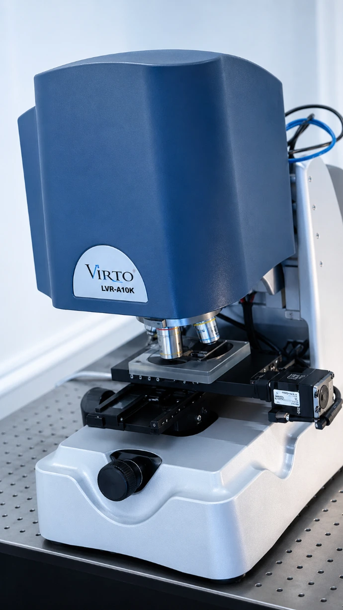
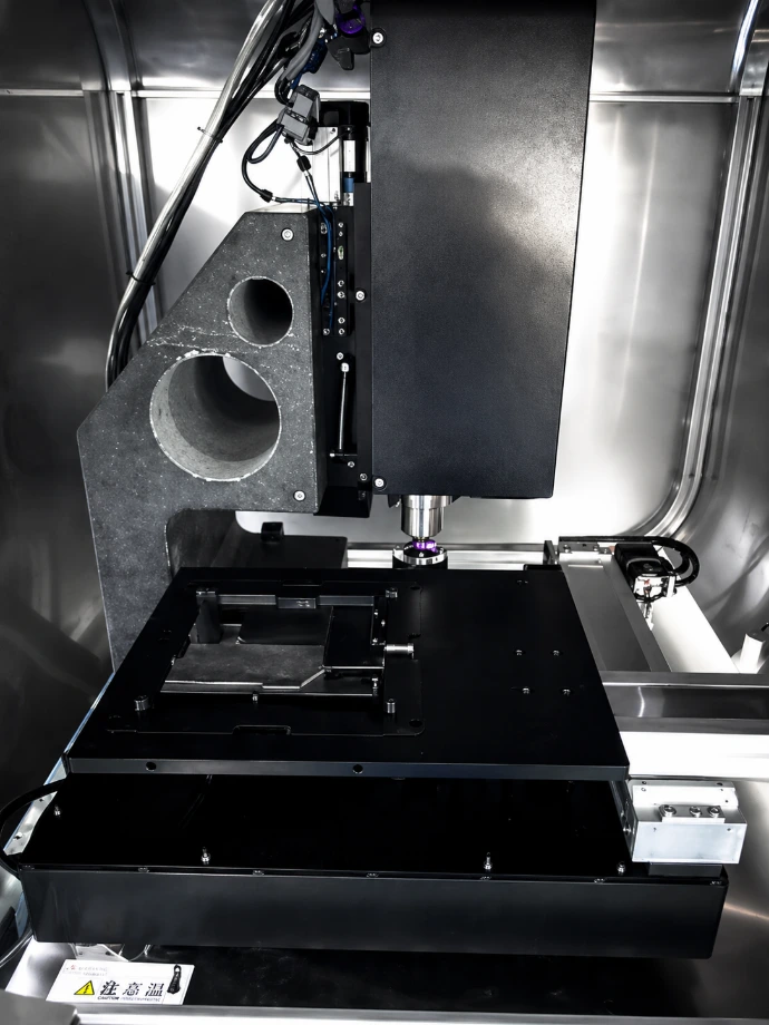
Quality Inspection Equipment
Equipped with professional optical measurement instruments to ensure every glass substrate meets the strictest quality standards in the semiconductor and optics industries.